Introduction To Ceramic Substrates
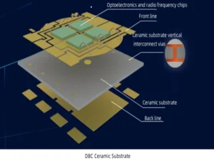
Ceramic substrates currently play a very important role in the field of electronic technology. The core is determined by the advantages of ceramic substrates such as high thermal conductivity, high insulation, and thermal conductivity. So what are the outstanding advantages of ceramic substrates and ceramic substrates?
The difference between ceramic substrate and ceramic substrate
Ceramic substrate is a sheet material based on electronic ceramics that forms a supporting base for membrane circuit components and external components.
Ceramic substrate refers to a special process board in which copper foil is directly bonded to the surface of the ceramic substrate (single or double-sided) at high temperature. The ultra-thin composite substrate made of ceramic substrate has excellent electrical insulation properties, high thermal conductivity, excellent solderability and high adhesion strength, and can be etched with various patterns like a PCB board, which has great potential. Current carrying capacity. Therefore, ceramic substrates have become the basic material for high-power power electronic circuit structure technology and interconnection technology.
In short, to put it simply, there are no circuits on the substrate, and metal circuits have been etched on the substrate.
Core advantages of ceramic substrates
The ceramic substrate has strong mechanical stress and stable shape; high strength, high thermal conductivity, and high insulation; strong bonding force and anti-corrosion; has excellent thermal cycle performance, with a cycle number of 50,000 times, and high reliability; and is compatible with PCB boards ( Or IMS substrate) can also etch various pattern structures; no pollution, no pollution.
Performance requirements of ceramic substrates:
- Mechanical properties
It has high enough mechanical strength and can also be used as a supporting member in addition to carrying components; it has good processability and high dimensional accuracy;
- Electrical properties
High insulation resistance and insulation breakdown voltage; Low dielectric constant; Dielectric loss is small; Stable performance under conditions of high temperature and high humidity, ensuring reliability.
- Thermal properties
High thermal conductivity; The thermal expansion coefficient matches the relevant material (especially the thermal expansion coefficient of Si); Excellent heat resistance.
- Other properties
Good chemical stability; easy to metallize, strong adhesion between circuit patterns and it; Non-hygroscopic; resistant to oil and chemicals; small amount of a-ray emission;The materials used are non-polluting and non-toxic; within the operating temperature range The internal crystal structure does not change
Ceramic Substrates Also Become Ceramic Circuit Boards, Ceramic Circuit Boards, Ceramic Pcb Boards, Etc.
Ceramic substrates can be divided into alumina ceramic substrates, aluminum nitride ceramic substrates, silicon nitride ceramic substrates, and silicon carbide ceramic substrates according to different ceramic substrate materials. etc., according to different processes, it can be divided into DPC ceramic substrate, DBC ceramic substrate, AMB ceramic substrate, HTCC ceramic substrate, LTCC ceramic substrate, etc.; according to the number of layers, it can be divided into single, double-sided ceramic substrate and multi-layer ceramic substrate. Ceramic substrates have good comprehensive electrical properties. Ceramic substrates serve more as a substrate, supporting, heat dissipating, and insulating.
Highlighted main advantages of ceramic circuit boards
- High thermal conductivity;
- More matching thermal expansion coefficient;
- Strong, low-resistance metal film layer;
- The base material has good weldability and high operating temperature;
- Good insulation;
- Low frequency loss;
- High-density assembly is possible;
- No organic components, resistant to cosmic rays, high aerospace reliability, and long service life;
- The copper layer does not contain an oxide layer and can be used for a long time in a reducing atmosphere.
Disadvantages of ceramic circuit boards
Fragility is the main disadvantage, which results in only small-area circuit boards being made.
The price is expensive, and there are more and more requirements and regulations for electronic products. Ceramic circuit boards are still used in some relatively high-end products, but are not used in low-end products at all.
Ceramic circuit board application range
Ceramic circuit boards can be used in LEDs, high-power semiconductor modules, semiconductor coolers, electronic heaters, power control circuits, power hybrid circuits, intelligent power components, high-frequency switching power supplies, solid-state relays, automotive fields in electronics, communications, aviation It can be said that fields such as aerospace and military electronic components occupy most areas of the electronics industry, and invisibly promote the development of the electronics industry.
Ceramic substrate refers to a special process board in which copper foil is directly bonded to the surface (single or double-sided) of aluminum oxide (Al2O3) or aluminum nitride (AlN) ceramic substrate at high temperature. The ultra-thin composite substrate produced has excellent electrical insulation properties, high thermal conductivity, excellent solderability and high adhesion strength, and can be etched with various patterns like a PCB board and has a large current carrying capacity. ability. Therefore, ceramic substrates have become the basic material for high-power power electronic circuit structure technology and interconnection technology.
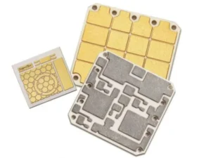
Ceramic Substrate Classification
Classification by manufacturing process:
Ceramic substrates are mainly divided into two categories: flat ceramic substrates and three-dimensional ceramic substrates.
The main flat ceramic substrate processes can be divided into thin film ceramic substrate (TFC), thick film printed ceramic substrate (TPC), direct bonded copper ceramic substrate (DBC), active metal welding ceramic substrate (AMB), direct electroplated copper ceramic substrate ( DPC).
The main three-dimensional ceramic substrates are divided into high-temperature co-fired ceramic substrates (HTCC) and low-temperature co-fired ceramic substrates (LTCC)
The more common types of ceramic heat dissipation substrates at this stage include: HTCC, LTCC, DBC, DPC, AMB, etc.
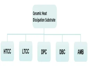
HTCC (High Temperature Co-fired Ceramic): It is an earlier developed technology. It is a multi-layer ceramic substrate obtained by co-firing ceramics with metal patterns such as W and Mo with high melting points. However, the high sintering temperature limits the choice of electrode materials and the production cost is relatively high, which has prompted the development of LTCC.
LTCC (Low Temperature Co-fired Ceramic): LTCC technology lowers the co-firing temperature to about 850°C. By stacking and co-firing multiple ceramic diaphragms printed with metal patterns, circuits can be routed in three-dimensional space. LTCC has outstanding advantages in the field of passive integration and is widely used in 3C, communications, automotive, military and other markets. It can realize the packaging of three major passive devices (resistors, capacitors, inductors) and various passive devices (such as filters, transformers, etc.) in multi-layer wiring substrates, and integrate them with active devices (such as power MOS, transistors, IC modules, etc.) are integrated into a complete circuit system (such as SiP). Now it is widely used in various types of mobile phones, Bluetooth, GPS modules, WLAN modules, WIFI modules, etc.; in addition, due to the high reliability of its products, it has been widely used in automotive electronics, communications, aerospace and military, micro-electromechanical systems, and sensor technology. Applications in other fields are also increasing.
DPC (Direct Plating Copper): It is a ceramic circuit processing technology developed on the basis of ceramic thin film processing. Ceramics are used as the circuit substrate, a metal layer is compounded on the surface of the substrate using a sputtering process, and the circuit is formed using electroplating and photolithography processes.
DBC (Direct Bonded Copper): A composite substrate is made by directly sintering copper foil to the surface of Al2O3 and AlN ceramics at high temperature through a hot-melt bonding method.
AMB (Active Metal Brazing): AMB is developed on the basis of DBC technology. At a high temperature of about 800°C, AgCu solder containing active elements Ti and Zr wets the interface between ceramic and metal. and react to achieve heterogeneous bonding between ceramics and metals.
In summary, among the above five major process types, HTCC\LTCC are all sintering processes, and the cost will be higher. DBC and DPC are professional technologies that have been developed and matured in China in recent years and can be mass-produced. DBC uses high-temperature heating to combine Al2O3 and Cu plates. The technical bottleneck is that it is not easy to solve the problem of micro-pores between Al2O3 and Cu plates. , which poses a greater challenge to the mass production energy and yield of this product. DPC technology uses direct copper plating technology to deposit Cu on the Al2O3 substrate. The process combines material and thin film process technology. Its products are The most commonly used ceramic heat sink substrate in recent years. However, its material control and process technology integration capabilities are relatively high, which makes the technical threshold for entering the DPC industry and achieving stable production relatively high.
Compared with traditional products, AMB ceramic substrate is bonded by chemical reaction between ceramic and active metal solder paste at high temperature. Therefore, its bonding strength is higher and its reliability is better. It is very suitable for connectors or those with large current carrying capacity. Scenarios with high heat dissipation requirements. In particular, power electronics and high-power electronic modules with stringent performance requirements such as new energy vehicles, rail transit, wind power generation, photovoltaics, and 5G communications have a huge demand for AMB ceramic copper clad laminates.
Classification by material:
The main materials of ceramic substrates include beryllium oxide (BeO), aluminum oxide (Al2O3), aluminum nitride (AlN) and silicon nitride (Si3N4), etc.
Ceramic powder is a key factor affecting the physical and mechanical properties of ceramic substrates. The purity, particle size, phase, oxygen content, etc. of the powder will have an important impact on the thermal conductivity and mechanical properties of the ceramic substrate. Its characteristics also determine the selection of the substrate forming process and sintering process.
BeO ceramic has high thermal conductivity, but its toxicity and high production cost limit its production and application.
Al2O3 ceramic substrate has been widely used because of its low price and good thermal shock resistance. However, due to its relatively low thermal conductivity and mismatched thermal expansion rate, it can no longer fully meet the development of power devices in the direction of high power and miniaturization. trend.
The advantages of AlN and Si3N4 ceramic substrates in terms of expansion coefficient and thermal conductivity are considered to be the future development direction. The flexural strength of Si3N4 has been greatly improved, and designers have benefited from this; its fracture toughness even exceeds that of zirconia-doped ceramics, reaching 6.5~7 MPa/√m at a thermal conductivity of 90 W/mK.
Future Growth And Market Analysis Of Several Major Ceramic Substrate Process Technologies
Future market analysis of HTCC ceramic substrates:
China is currently the world’s largest consumer market, accounting for 26.8% of the market in 2022, followed by North America, Japan and Europe, accounting for 17%, 16.0% and 15.8% respectively. It is expected that China will grow the fastest in the next few years.
Global HTCC market sales will reach 19.6 billion yuan in 2022, and are expected to reach 28.9 billion yuan in 2029, with a compound annual growth rate (CAGR) of 5.67% (2023-2029).
From a regional perspective, the Chinese market has changed rapidly in the past few years. The market size in 2022 will be 5.2 billion yuan, accounting for approximately 26.8% of the global market. It is expected to reach 9.19 billion yuan in 2029, when the global share will reach 31.7%.
Future market analysis of LTCC ceramic substrates:
5G communications puts forward technical development requirements for terminal electronic components such as miniaturization, lightweight, low cost, and high performance. LTCC has the advantages of low cost, diverse and flexible designs, and excellent high-frequency microwave performance. It can be applied in the era of 5G and the Internet of Everything. Various application scenarios and high-frequency communication mobile terminals, including automotive electronics, computers, telemedicine, smart homes, high-frequency communications, etc. The development of high-performance LTCC products will become an urgent need in the era of 5G and the Internet of Everything. In the future, with the development of 5G applications, Internet of Everything and other markets, domestic demand for LTCC products will further increase. According to Guanyan Tianxia’s prediction, the domestic LTCC market size will reach 9.038 billion yuan by 2025.
DBC ceramic substrate future market analysis:
According to statistics and forecasts from APO, the global DBC ceramic substrate market sales will reach US$403 million in 2022, and are expected to reach US$767 million in 2029, with a compound annual growth rate (CAGR) of 9.71% (2023-2029 ).
The core manufacturers of global DBC Ceramic Substrate include Rogers Corporation, Ferrotec, KCC, Hefei Shengda, Heraeus, etc. The top five manufacturers account for approximately 80% of the global market share. Asia-Pacific is the largest market, with a share of approximately 68%, followed by Europe and North America, with shares of 24% and 7% respectively. In terms of product types, alumina and ZTA DBC ceramic substrates are the largest segments, accounting for about 85% of the market share. In terms of downstream products, new energy vehicles are the largest downstream field, accounting for 59% of the market share.
At present, the upstream ceramic powders and white boards of DBC ceramic substrates are mainly dominated by Japanese manufacturers. At present, domestic manufacturers occupy an important share in aluminum nitride ceramic substrate whiteboards and alumina ceramic substrate whiteboards, but in the high-end field, Japanese manufacturers are still dominant.
DPC ceramic substrate future market analysis:
The global DPC ceramic substrate market size will be US$260 million in 2022, and is expected to reach US$273 million in 2023. DPC ceramic packaging substrates are more in line with the future development direction of high density, high precision and high reliability. The global DPC ceramic substrate market will continue to grow in the next few years.
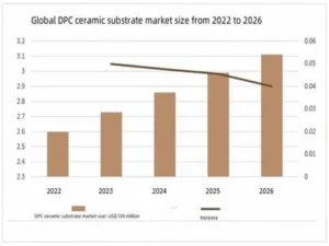
DPC ceramic substrates are mainly used in the LED field, accounting for 69%. There are many DPC ceramic substrate manufacturers in the world, and the TOP4 companies account for 59% of the global DPC ceramic substrate market.
AMB ceramic substrate future market analysis:
At present, aluminum nitride ceramic substrates using the AMB process (AMB-AlN) are mainly used in high-voltage and high-current power semiconductors such as high-speed rail, high-voltage converters, and DC power transmission; silicon nitride ceramic substrates using the AMB process (AMB-SiN ) are mainly used in electric vehicle (EV) and hybrid vehicle (HV) power semiconductors. In the next few years, silicon nitride ceramic substrates (AMB-SiN) are expected to grow more rapidly. [AMB Ceramic Substrate] Thanks to the strong demand for new energy vehicles, the demand for power modules has grown rapidly, increasing the demand for AMB ceramic substrates; in addition, new energy power generation, especially photovoltaics, wind power, etc., under the background of the Russia-Ukraine war, energy Security is one of the core concerns of important countries around the world and will maintain rapid growth.
As SiCMOS begins to supply main drive inverters, the production capacity consumption of ceramic substrates increases rapidly as the SiCMOS area required for the inverter increases. The penetration rate of silicon carbide vehicle models is expected to increase rapidly in 2024, and the new energy vehicle field will become the largest demand area for AMB ceramic substrates. Among them, the global AMB ceramic substrate market sales will reach US$433 million in 2022, and are expected to reach US$2.872 billion in 2029, with a compound annual growth rate (CAGR) of 26.0% (2023-2029). After the AMB ceramic substrate industry researches new technologies, it is expected to reach 17.4 billion yuan in 2029.
